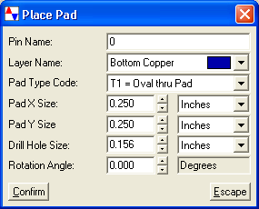
Pad Types Codes and definitions:
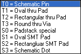 | |
| T0 = Schematic Pin | Not used in a PCB |
| T1 = Oval thru Pad | Copper on both the top and the bottom, drill hole, solder mask relief, and rounded corners. |
| T2 = Rectangular thru Pad | Copper on both the top and the bottom, drill hole, solder mask relief, and square corners. |
| T3 = Round thru Via | Copper on both the top and the bottom, drill hole, no solder mask relief, and rounded corners. |
| S0 = Padstack special | Data on only the assigned layer, drill hole, rounded corners. |
| S1 = Oval SMT Pad | Copper on only the assigned layer, no drill hole, solder mask relief, solder paste relief, and rounded corners. |
| S2 = Rectangular SMT Pad | Copper on only the assigned layer, no drill hole, solder mask relief, solder paste relief, and square corners. |
| S3 = Schematic Dot | Not used in a PCB. |