Building your first board (Schematic Section)
Step 1:
Invoke CIRCAD and select New from the File menu.
Step 2:
From the Schematic Files group box select Size A, and then click Confirm.
Step 3:
CIRCAD will open the File Save As... dialog box giving you an opportunity to save the new file that you have just created. Enter a new name into the File Name
filed and click Confirm.
Step 4:
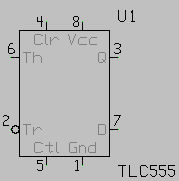
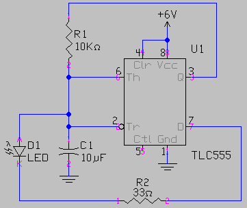
For our example we will build a small, efficient LED flasher. Select Component from the Place menu or type the keys <PC>. In the Pattern: field
type TLC555 and press enter. You will see a preview of the component in the window below. You may notice that it has been assigned a Reference Identifier (Ref ID:) of U1
and defined the PCB Pattern: to be a DIP8. Click Confirm and select a central location on the schematic sheet to place the part.
Step 5:
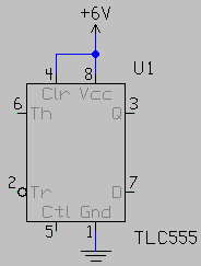
Now let's hook up power. Press the <L> key. This will pop up a list of the layers. Select the Master layer either by clicking on it in the dialog box or by
pressing the <0> key (since it is on layer number 0). Zoom in on the part (zoom in with the <I> key and out with the <O> key) and locate
the green pad on the end of pin number 8.

These green pads are where you will be connecting your wires to the component. If the Pin names/numbers option is selected in the Setup Draw Modes
(<SM>) dialog box there will be a purple number 8 directly on top of it (I have disabled this option for this part of the example). With the crosshairs active
(crosshairs may be invoked and released by pressing the space bar) roll over the green pad and type <PW> for Place Wire. Now, roll up 200 mils and click to
set the new wire down. If you continue to roll you will notice that a new "ghost wire" has been attached to the cursor for the placing of additional lines. Since we are done
with this particular line segment we will escape from the ghost line by either pressing the Escape key, or right clicking the mouse. At the top end of the wire that
we have just created, type <P+> for Place +/- Port. A dialog box will appear prompting you to enter a signal name for your new power port. Enter +6V and
click Confirm. You will see an arrow and a piece of text that reads &@ ghosted and attached to the cursor. If you are not on the upper endpoint of the line that we
just created, roll there now and click to set down the power port. You will notice that the &@ now reads +6V. Next roll over pin number 4 and again (in crosshair mode of course)
type <PW> and roll up 100 mils and click to set this line segment down. Now roll right 200 mils and click again to set this segment's end point on top of the first
line that we created. At the junction of the two lines place a schematic dot with the Place Dot function (<PD>) to ensure that the two segments are joined.
You should have something that looks like this:
Step 6:
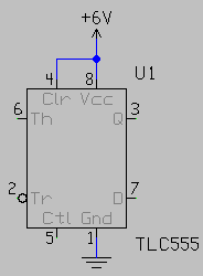
Ground comes next. Roll down to pin 1 and locate its pad. Roll over the pad a type <PW>, and then roll down 100 mils and click to set this line segment down. Now
type <PG> for Place GND and click to set it down. While electrical continuity could be achieved by placing the pad of the ground component directly onto the
pad of pin 1, the process described above yields better looking results, while maintaining connection if either of the two parts is moved by "rubber banding" the intervening
line segment.
Step 7:
Let's place some more components. While the ICs have pin numbers built into their drawing, many of the discreet components don't, so if it's not already on, let's turn on our
Pad pin numbers display. To do this type <SM> for
Setup Draw Modes. In the --- Tags --- section, check the Pad pin numbers box and click Confirm.
Now type <PC>, and in the Pattern: field type <R*> (R asterisk) and press and enter. The list on the right will show all of the components that
start with the letter R. Clicking on any of the parts will show a preview of it. The list may be traversed by either clicking on individual items or by using the up and down
arrow keys. Let's select the first resistor in the list which is named R and has a description of Generic[vertical]. You will notice that the component has a
Ref ID: of R1. This number is automatically assigned and can be changed as desired. Because it is a new part, it has a Type/Value of ?Ohms. Click in the
Type/Value field and enter 10KOhms. Next click in the PCB Pattern: field. Since It already reads R*, simply press enter. The list will now show all PCB components
that start with the letter R. Select the first one, R300P60 Eighth watt. Now that our new schematic resistor is ready for placement, click Confirm. The resistor
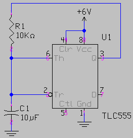
will be ghosted and attached to the cursor. Place it such that pin 2 is 100 mils up from pin 6 of the TLC556 and slightly to the left (I placed mine 400 mils left). Now place
a 10µF cap with pin 1 100 mils down from pin 2 of the TLC555 directly under the previous resistor. To do this type <PC>, and enter C* for the Pattern: and
select the Generic[vertical] cap. Enter 10µF into the Type/Value:, and then click on the PCB Pattern: field and press enter to search for all PCB components
that start with C. Chose the PCB Pattern: that you like and click Confirm (I chose C100/150 tantalum). Let's wire up what we have done before we place the rest of
the parts. First, place a wire between pin 1 of the cap and pin 2 of the resistor using the <PW> function. Second, place a wire from pin 6 of the TLC555 right, up,
left, and down to pin 1 of the resistor. Next, place a wire from pin 6 of the TLC555 to the wire that connects the resistor and the cap and place a schematic dot over the
intersection using the Place Dot function (<PD>). Now place a wire from pin 2 of the TLC555 to the wire that connects the resistor and cap, and again place
a dot over the intersection. The reason the we place the resistor and the cap 100 mils up and down from their corresponding pins on the TLC555 is so that we wouldn't have to
place the dot on top of the pin for the cap and resistor (while this would be functionally acceptable it's just a little tacky). Place a ground (<PG>) 100 mils
below pin 2 of the cap and connect it with a short wire like you did with the ground on the TLC555. Let's take a look at what we have so far:
Step 8:
Using the Place Component function, place a LED (name: LED, description: Light emitting[vertical]) next to the cap. Also place a Generic[horizontal] 33Ohms resistor below
pin five of the TLC555. Place a dot above the one that connects the resistor and the cap to the TLC555. Place a wire from the new dot to the anode of the LED (pin number A).
Wire the cathode (pin number K) to pin 1 of the horizontal resistor. Connect pin 2 of the horizontal resistor to pin 7 of the TLC555. Here is a sample of what you should have:
Step 9:
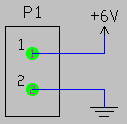
Almost done! Now that our basic circuit is complete we have just two tasks to complete. First we have to get power and ground into our circuit. To do this use the Place
Component function to place a small connector (I chose to use a SIP2). Wire one pin to ground and the other pin to power just like we did in the beginning of Step 5
(<P+>, enter +6V, click Confirm, set it on the wire to the pin of the connector). It is always good to update the data in the Title Block in the lower right
corner of the drawing. Later on, this data could be automatically generated by customizing the template files (see Chapter 12
of the online manual). If you chose the same connector that I did then it will look something like this:
Last step for the schematic:
The schematic is now complete. Before we continue, you should save the file to disk just in case someone comes along and trips over the power cord. Type <NO> for
the Netlist Out function. A dialog box will appear asking for a path for the netlist. This will be the path of the schematic. It will also ask for Circad or Tango format
netlist. Select the options and path that you want and click Confirm. Now onto the PCB!